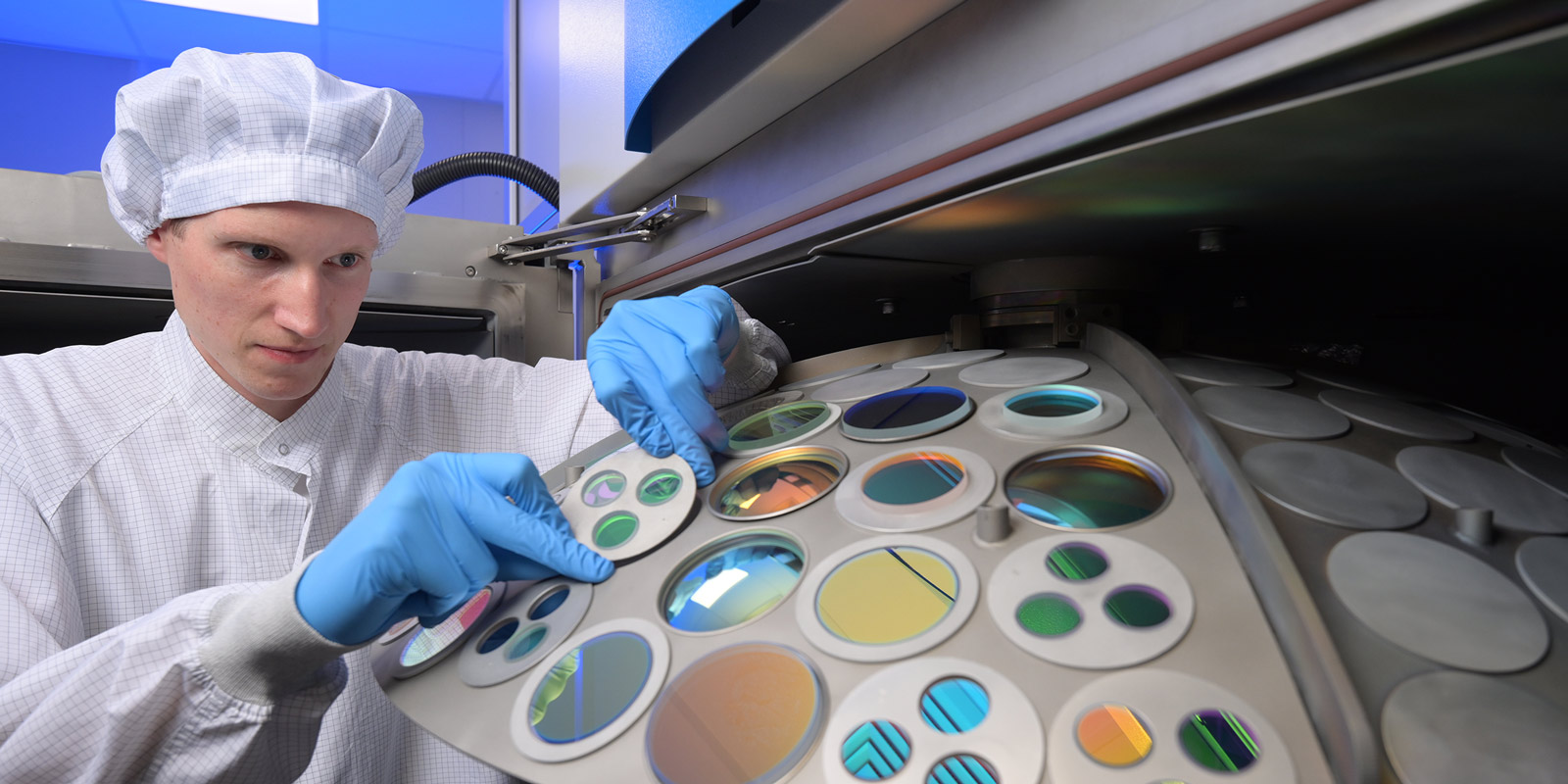
LASER - World of PHOTONICS 2023: Optical Components

Contact
Phone: +49 511 2788-419
Email: messe@lzh.de
Smart Optical Coatings
Motivation
• Production of high-end optical components
• Functionalization of surfaces with optical coatings
• Flexible optical & mechanical properties
• Protection layers
Function/Properties/ Characteristics
• Various processes for all sample types'
• Ion Beam sputtering for high-precision coatings
• Atomic layer deposition for free-form components
• Thermal processes for expanded material range
Applications
• High-power applications
• Precision metrology
• Integrated optical systems

rALD Coatings
Motivation
• Rising form complexity of optics
• CNC milling, polishing
• 3D printed, injection molding, casting
• Need of conformal coatings
• Sensitive materials
Function/Properties/ Characteristics
• High conformal, low temperature coatings
• Large areas up to 200 mm diameter
• Low spectral absorption
Applications
• Planar and non-planar optics
• Aspheres, Fresnel lenses, prisms
• Gratings
• Capsuling
• e.g. laser crystals
Parameters
• ~0.14 nm/sec growth rate
• 150°C deposition temperature
Processed material
• 200 nm Ta2O5
• 8’’ silicon wafer
Sample loading
• Direct or via load lock
Outstanding growth rate
• Up to 1000 nm/h
• Temperature range 25-200°C
Batch size
• 7 pieces 200 mm
• 13 pieces 100 mm
• 384 pieces 25 mm


IBS Coatings
• Highest coating precision, nearly perfect thin film structure
• „Cold“ deposition process (< 80 °C)
• Sputtering of the target material, substrates are deposited with sputtered particles
• Oxides, (fluorides), metals
• Applications: DUV, UV / VIS-IR, high fs-LIDT


Miniaturized optical thin film filters
• High-precision IBS coating on wafer with sacrificial substrate
• Laser cutting into single filter elements
• Transfer to tape via dissolving sacrificial substrate
• Filter edge length 25 µm up to 1 mm with rectangular or freeform shape
• Miniaturization allows for high integration density in hybrid photonic systems or telecom fiber applications
• Substrate-free technique enables low loss integration between waveguides or fibers

High Resolution Optical Broadband Monitoring
Motivation
• Precise in situ coating thickness monitoring for production of optical thin-film filters
Function
• Direct broadband measurement of moving substrates on rotating substrate holder in UV to NIR wavelength range
Applications
• Precise deposition control
• Online characterization of coatings
• Automated process control
• Rapid manufacturing of complex optical designs
• Faster development of new coating processes
• Quality control and documentation of production processes
• Increased process yield using advanced simulation, re-optimization and error handling tools
• Modular system, flexible configuration according to customer specification in wavelength range and resolution
Technical data
| BBM | HR BBM | |
| Wavelength range | 240 - 1000 nm optional IR: 240 - 1700 nm |
|
| Spectral resolution | 1 - 1.5 nm IR: 1 - 5 nm |
0.1 - 0.2 nm IR: 0.1 - 3 nm |
| Measurement time | 10 µs - 30 ms | |
| Wavelength accuracy | < 0.5 nm | |
| Reproductibility of 100%-measurement | better ±0.04% | |
| Noise of 100%-measurement | < 1% RMS | |
Performance and Options
• Software algorithms for data acquisition, thickness determination and process control
• BBM simulation module, including a virtual deposition unit: advanced design stability analysis
• Re-optimization module: online error analysis and automated design refinement for increased yield
• Modular system: options for uniformity measurements on multiple radii, combined transmittance and reflectance measurements, spectral resolution below 1 nm (High Resolution / HR BBM)
• In addition to the standard configuration, customized adaptions, e.g. for spectral range and resolution, are available
Applicability
• System compatibility to nearly all deposition chambers and customer specified instrumentation
• Best applicability to IAD and sputter deposition processes